
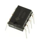
PRECISION TIMER, SINGLE, 500kHz, 16V, DIP-8
Description:
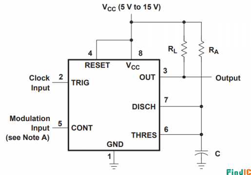
Ti NE555P is precision timing circuits capable ofproducing accurate time delays or oscillation. In thetime-delay or mono-stable mode of operation, thetimed interval is controlled by a single externalresistor and capacitor network. In the a-stable modeof operation, the frequency and duty cycle can becontrolled independently with two external resistorsand a single external capacitor.
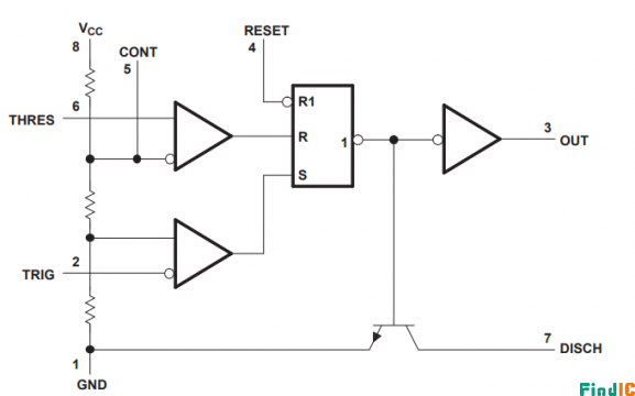
The threshold and trigger levels normally are two-thirds and one-third, respectively,of VCC.Theselevels can be altered by use of the control-voltageterminal. When the trigger input falls below the trigger
level, the flip-flop is set, and the output goes high. Ifthe trigger input is above the trigger level and thethreshold input is above the threshold level, the flip-flop is reset and the output is low. The reset (RESET)input can override all other inputs and can be used toinitiate a new timing cycle. When RESET goes low,the flip-flop is reset, and the output goes low. Whenthe output is low, a low-impedance path is providedbetween discharge (DISCH) and ground.
The output circuit is capable of sinking or sourcingcurrent up to 200 mA. Operation is specified forsupplies of 5 V to 15 V. With a 5-V supply, outputlevels are compatible with TTL inputs.
Timing From Microseconds to Hours
Astable or Monostable Operation
Adjustable Duty Cycle
TTL-Compatible Output Can Sink or SourceUp to 200 mA
On Products Compliant to MIL-PRF-38535,All Parameters Are Tested Unless OtherwiseNoted. On All Other Products, ProductionProcessing Does Not Necessarily thirds and one-third, respectively, of VCC. These IncludeTesting of All Parameters.
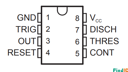
Pin 1(ground): ground wire (or common ground), usually connected to the circuit common ground.
pin 2(trigger point): this pin bit is the time period that triggers NE555 to start it. The upper edge voltage of the trigger signal shall be greater than 2/3 VCC, the lower edge shall be less than 1/3 VCC.
Pin 3(output): the output pin of 555 starts at the time period and moves to a high potential of 1.7 volts less than the supply voltage. The end output of the cycle returns to a low potential of about 0 volts. A maximum output current of about 200 mA. at high potential
Pin 4(reset): a low logic potential is sent to this pin bit to reset the timer and return the output to a low potential. It is usually connected to a positive power supply or ignored.
Pin 5(Control): this pin allows the trigger and gate voltage to be changed by external voltage. This input can be used to change or adjust the output frequency when the timer operates in a stable or oscillating mode.
pin 6(reset lock): reset lock and make output low. Start this action when the pin voltage moves from 1/3 VCC below the voltage to more than 2/3 VCC.
Pin 7(discharge): this pin and the main output pin have the same current output capability, LOW, to ground is low impedance when the output is 0 N, and HIGH, to ground is high impedance when the output is 0 FF.
pin 8(V): this is the positive supply voltage end IC 555 timers. The supply voltage ranges from 4.5 volts (minimum) to 16 volts (maximum).
Technical parameters:
Frequency :500 kHz
Supply voltage (DC):4.50 V (min)
rated current: A 10.0
Output current :200 mA
Current :10 mA
Number of pins :8
Static current: mA 2.00
Operating temperature (Max):70℃
Operating temperature (Min):0℃
Power supply :4.5 V ~16 V
Supply voltage (Max):16V
Supply voltage (Min):4.5V
Package parameters:
Installation: Through Hole
Number of pins :8
Encapsulation: DIP-8
Dimensions:
Length: mm 9.81
Width: mm 6.35
Height: mm 4.57
Encapsulation: DIP-8
Physical parameters:
Working temperature :0℃~70℃
Other:
Product life cycle: Active
Packing: Tube
Manufacturing applications: Consumer Electronics, embedded design and development, Defence,Clock &Timing, defense, clock and timing, military and aviation, consumer electronics, Aerospace,Embedded Design &Development,Military
Compliance:
RoHS criteria: RoHS Compliant
Criteria for Lead: Lead Free
REACH SVHC criteria: No SVHC
Military grade: Yes
ingerprint Biometrics
lris Biometrics
RFID Reader