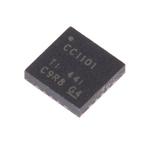
FindIC - A Global Electronic Components Search Engine
Categories
IC Testing Lab AiBOM
English
Home > Popular Part No. >

CC1101 Series Datasheet

CC1101

Wireless data transmission chip

CC1101 is a wireless data transmission chip produced by the American TI company that works in the sub-1GHz frequency band. It is a sub-1GHz design aimed at extremely low-power RF applications. It is mainly aimed at industry, scientific research and medical (ISM) and short-range wireless communication equipment (SRD). CC1101 can provide extensive hardware support for data packet processing, data buffering, burst transmission, received signal strength indicator (RSSI).

CC1101 Pin Configuration and Function

image.png


Pin Number

Pin Name

Description

1

SCLK

Serial   configuration interface, clock input

2

SO (GDO1)

Serial   configuration interface, data output. Optional general output pin   when   CSn is high

3

GDO2

Digital output   pin for general use:Test signals/FIFO status   signals/Clear channel   indicator/Clock output, down-divided from XOSC/Serial   output RX data

4

DVDD

1.8 - 3.6 V   digital power supply for digital I/O’s and for the   digital core voltage regulator.

5

DCOUPL

1.6 - 2.0 V   digital power supply output for decoupling.NOTE: This pin is   intended   for use with the CC1101  only.   It can not be used to provide   supply voltage to other devices.

6

GDO0(ATEST)

Digital output   pin for general use:Test signals/FIFO status   signals/Clear channel   indicator/Clock output, down-divided from XOSC/Serial   output RX data   /Serial input TX data/Serial output RX data.Also used as   analog test   I/O for prototype/production testing

7

CSn

Serial   configuration interface, chip select

8

XOSC_Q1

Crystal   oscillator pin 1, or external clock input

9

AVDD

1.8 - 3.6 V   analog power supply connection

10

XOSC_Q2

Crystal   oscillator pin 2

11

AVDD

1.8  - 3.6   V analog power supply   connection

12

RF_P

Positive RF   input signal to LNA in receive mode.Positive RF output   signal from PA   in transmit mode

13

RF_N

Negative RF   input signal to LNA in receive mode.Negative RF output   signal from PA   in transmit mode

14

AVDD

1.8 - 3.6 V   analog power supply connection

15

AVDD

1.8 - 3.6 V   analog power supply connection

16

GND

Analog ground   connection

17

RBIAS

External bias   resistor for reference current

18

DGUARD

Power supply   connection for digital noise isolation

19

GND

Ground connection   for digital noise isolation

20

SI

Serial   configuration interface, data input


CC1101 Series Datasheet

Part No
Picture
Manufacturer
Package
Description
Datasheet
CC1101RGPR
CC1101RGPR
TI
QFN

RF Transceiver IC, Sub 1GHz, 2FSK, 4FSK, ASK, GFSK, MSK, OOK, 600Kbps, 1.8V to 3.6V, QFN-20

CC1101RGPT
CC1101RGPT
TI
VQFN-20

RF transceiver; 868MHz,315MHz,433MHz,915MHz; 1.8÷3.6VDC; SMD

CC1101DK433
CC1101DK433
TI
-

Development Kit, Low Cost Low Power Sub 1GHz RF Transceiver, 433MHz, (2x) Antennas

CC1101RTKR
CC1101RTKR
TI
QFN

RF Transceiver ASK/FSK/GFSK/OOK/MSK 2.5V/3.3V 20Pin VQFN EP T/R

CC1101RGP
CC1101RGP
TI
VQFN-20

RF Transceiver ASK/FSK/GFSK/OOK/MSK 2.5V/3.3V 20Pin QFN Tube

FindIC user feedback
Question type
Website page questions or suggestions
Data problems or errors
Inquiry for component procurement
other
Comments and suggestions
Contact information
Feedback and contact