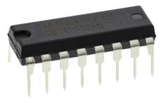
FindIC - A Global Electronic Components Search Engine
Categories
IC Testing Lab AiBOM
English
Home > Popular Part No. >

74LS138 Series Datasheet

74LS138

Logic chip

74LS138 is a member from ‘74xx’family of TTL logic gates. The chip is designed for decoding or de-multiplexing applications and comes with 3 inputs to 8 output setup. The design is also made for the chip to be used in high-performance memory-decoding or data-routing applications, requiring very short propagation delay times. In high performance memory systems these decoders can be used to minimize the effects of system decoding.

74LS138 Pin Configuration and Function

74LS138 Pin Configuration and Function

Pin Number

Pin Name

Description

1

A

Address input pin

2

B

Address input pin

3

C

Address input pin

4

G2A

Enable input (active LOW)

5

G2B

Enable input (active LOW)

6

G1

Enable input (active HIGH)

7

Y7

Output pin 7

8

GND

Ground

9

Y6

Output pin 6

10

Y5

Output pin 5

11

Y4

Output pin 4

12

Y3

Output pin 3

13

Y2

Output pin 2

14

Y1

Output pin 1

15

Y0

Output pin 0

16

VCC

Power supply pin


74LS138 Series Datasheet

Part No
Picture
Manufacturer
Package
Description
Datasheet
SN74LS138N
SN74LS138N
TI
SOIC, PDIP

TEXAS INSTRUMENTS SN74LS138N Decoder / Demultiplexer, LS Family, 3:8, 4.75V to 5.25V, DIP-16

SN74LS138D
SN74LS138D
TI
SOIC, PDIP

TEXAS INSTRUMENTS SN74LS138D Decoder / Demultiplexer, LS Family, 3:8, 4.75V to 5.25V, SOIC-16

SN74LS138DR
SN74LS138DR
TI
SOIC

Decoder / Demultiplexer, LS Family, 8 Output, 4.75V to 5.25V, SOIC-16

SN74LS138M
ON Semiconductor
-

Decoder/Demultiplexer Single 3-to-8 16Pin SO EIAJ

FindIC user feedback
Question type
Website page questions or suggestions
Data problems or errors
Inquiry for component procurement
other
Comments and suggestions
Contact information
Feedback and contact