Pin Number | Pin Name | Description |
1 | COMP | DAC Bias Pin. This pin is used for decoupling the DAC bias voltage. |
2 | VDD | Positive Power Supply for the Analog and Digital Interface Sections. The on-board 2.5 V regulator is also supplied from VDD. VDD can have a value from 2.3 V to 5.5 V. A 0.1 μF and a 10 μF decoupling capacitor should be connected between VDD and AGND. |
3 | CAP/2.5V | The digital circuitry operates from a 2.5 V power supply. This 2.5 V is generated from VDD using an on-board regulator when VDD exceeds 2.7 V. The regulator requires a decoupling capacitor of 100 nF typical, which is connected from CAP/2.5V to DGND. If VDD is less than or equal to 2.7 V, CAP/2.5V should be tied directly to VDD. |
4 | DGND | Digital Ground. |
5 | MCLK | Digital Clock Input. DDS output frequencies are expressed as a binary fraction of the frequency of MCLK. The output frequency accuracy and phase noise are determined by this clock. |
6 | SDATA | Serial Data Input. The 16-bit serial data-word is applied to this input. |
7 | SCLK | Serial Clock Input. Data is clocked into the AD9833 on each falling edge of SCLK. |
8 | FSYNC | Active Low Control Input. FSYNC is the frame synchronization signal for the input data. When FSYNC is taken low,the internal logic is informed that a new word is being loaded into the device. |
9 | AGND | Analog Ground. |
10 | VOUT | Voltage Output. The analog and digital output from the AD9833 is available at this pin. An external load resistor is not required because the device has a 200 ? resistor on board. |

* Digitally programmable frequency and phase * 12.65mW power consumption at 3V * 0 MHz to 12.5MHz output frequency range * 28Bit resolution: 0.1Hz at 25MHz reference clock * Sinusoidal, triangular, and square wave outputs * 2.3V to 5.5V power supply * No external components required * 3-wire SPI interface * Extended temperature range:-40℃ to +105℃ * Power-down option * 10-lead MSOP package * Qualified for automotive applications

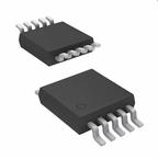
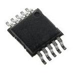
Direct Digital Synthesizer 25MHz 1DAC 10Bit Serial 10Pin MSOP T/R

Direct Digital Synthesizer 25MHz 1DAC 10Bit Serial 10Pin MSOP T/R

Direct Digital Synthesizer 25MHz 1DAC 10Bit Serial (3-Wire, SPI) 10Pin MSOP T/R