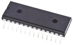
Pin Number | Pin Name | Description |
1~5, 26~28 | IN0~IN7 | 8 analog inputs |
6 | START | A/D conversion start pulse input terminal, input a positive pulse (at least 100ns wide) to start (the rising edge of the pulse resets 0809, and the falling edge starts the A/D conversion). |
7 | EOC | The A/D conversion end signal is output. When the A/D conversion ends, this end outputs a high level (it is always a low level during the conversion period). |
8, 14, 17~21 | 2-1~2-8 | 8-bit digital output |
9 | OUTPUT ENABLE | Data output permission signal, input, active high. When the A/D conversion is over, input a high level at this end to open the output three-state gate and output the digital quantity. |
10 | CLOCK | Clock pulse input terminal. The clock frequency is required to be no higher than 640KHZ. |
11 | Vcc | Power supply, single +5V. |
12 | Vref(+) | The reference voltage |
13 | GND | Ground |
16 | Vref(-) | The reference voltage |
23~25 | ADDC、ADDB、ADDA | 3-bit address input line, used to strobe one of the eight analog inputs |
22 | ALE | Address latch enable signal, input, active high. |
8Bit Microprocessor Compatible A/D Converters With 8Channel Multiplexer 28-PDIP -40℃ to 85℃
IC, ADC, 8Bit, 10KSPS, DIP-28
8Bit Microprocessor Compatible A/D Converters With 8Channel Multiplexer 28-PDIP -40℃ to 85℃
8Bit Microprocessor Compatible A/D Converters With 8Channel Multiplexer 28-PLCC -40℃ to 85℃