Pin Number | Pin Name | Description |
1 | RO | Receiver Output. If A > B by 200mV, RO will be high; if A < B by 200mV,RO will be low. |
2 | RE | Receiver Output Enable. RO is enabled when RE is low; RO is high imped-ance when REis high. If REis high and DE is low, the device will enter alow-power shutdown mode. |
3 | DE | Driver Output Enable. The driver outputs are enabled by bringing DE high.They are high impedance when DE is low. If RE is high and DE is low, the device will enter a low-power shutdown mode. If the driver outputs are enabled, the parts function as line drivers. While they are high impedance, they function as line receivers if RE is low. |
4 | DI | Driver Input. A low on DI forces output Y low and output Z high. Similarly, ahigh on DI forces output Y high and output Z low. |
5 | GND | Ground |
6 | A | Noninverting Receiver Input and Noninverting Driver Output |
7 | B | Inverting Receiver Input and Inverting Driver Output |
8 | Vcc | Positive Supply: 3.0V ≤VCC≤3.6V. Do not operate device with VCC> 3.6V. |

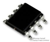
RS-422/RS-485 인터페이스 IC 3.3V 12Mbps Transceiver, 8-SOIC

Single Transmitter/Receiver RS-422/RS-485 8Pin SOIC N

1/1 Transceiver Half RS422, RS485 8-SOIC

Single Transmitter/Receiver RS-422/RS-485 8Pin SOIC N

Single Transmitter/Receiver RS-422/RS-485 8Pin SOIC N T/R